 |
参考报价:电议 型号:
产地:德国 在线咨询
|
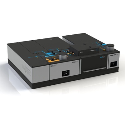
超高分辨散射式近场光学显微镜 - neaSNOM
产品简介:
neaSNOM是德国neaspec公司推出的第三代散射式近场光学显微镜(简称s-SNOM),其采用了**化的散射式核心设计技术,极大的提高了光学分辨率,并且不依赖于入射激光的波长,能够在可见、红外和太赫兹光谱范围内,提供优于10nm空间分辨率的光谱和近场光学图像。由于其高度的可靠性和可重复性,neaSNOM业已成为纳米光学领域热点研究方向的**科研设备,在等离基元、纳米FTIR和太赫兹等众多研究方向得到了许多重要科研成果。
*近,neaspec公司成功开发了可见至太赫兹高分辨光谱和成像综合系统,将上述s-SNOM功能与纳米红外(FTIR)、针尖增强拉曼(TERS)、超快光谱(ultrafast)和太赫兹光谱(THz)进行联用,可以为广大科学工作者在等离子激元、二维材料声子极化、半导体载流子浓度分布、生物材料红外表征、电子激发及衰减过程等的研究上提供相关支持。
技术特点和优势:
neaSNOM是目前世界上非常成熟的s-SNOM产品 **保护的散射式近场光学测量技术 —独有的极高10 nm空间分辨率 **的高阶解调背景压缩技术 —在获得10nm空间分辨率的同时保持极高的信噪比 专利保护的干涉式近场信号探测单元?**的赝外差干涉式探测技术 —能够获得对近场信号强度和相位的同步成像 | **保护的反射式光学系统 —用于宽波长范围的光源:可见、红外以至太赫兹 高稳定性的AFM系统 —同时优化了纳米尺度下光学测量 双光束设计 —极高的光学接入角:水平方向180°,垂直方向60° 操作和样品准备简单 —仅需要常规的AFM样品准备过程 |
重要应用领域:
部分发表文章:
Science (2017) doi:10.1126/science.aan2735 |
Tuning quantum nonlocal effects in graphene plasmonics |
Nature Nanotechnology (2017) doi:10.1038/nnano.2016.185 |
Acoustic terahertz graphene plasmons revealed by photocurrent nanoscopy |
Nature Photonics (2017) doi:10.1038/nphoton.2017.65 |
Imaging exciton–polariton transport in MoSe2 waveguides |
Nature Materials (2016) doi:10.1038/nnano.2016.185 |
Acoustic terahertz graphene plasmons revealed by photocurrent nanoscopy |
Nature Materials (2016) doi:10.1038/nmat4755 |
Thermoelectric detection and imaging of propagating graphene plasmons |
国内用户发表文章:
Nat. Commun. 8, 15561(2017) |
Imaging metal-like monoclinic phase stabilized by surface coordination effect in vanadium dioxide nanobeam |
Adv. Mater. 29, 1606370 (2017) |
The Light-Induced Field-Effect Solar Cell Concept –Perovskite Nanoparticle Coating Introduces Polarization Enhancing Silicon Cell Efficiency |
Light- Sci & Appl 6, 204 (2017) |
Effects of edge on graphene plasmons as revealed by infrared nanoimaging |
Light- Sci & Appl,中山大学accepted (2017) |
Tailoring of electromagnetic field localizations by two-dimensional graphene nanostructures |
Nanoscale 9, 208 (2017) |
Study of graphene plasmons in graphene–MoS2 heterostructures for optoelectronic integrated devices |
Nano-Micro Lett. 9,2 (2017) |
Molybdenum Nanoscrews: A Novel Non-coinage-Metal Substrate for Surface-Enhanced Raman Scattering |
J. Phys. D: Appl. Phys. 50, 094002 (2017) |
High performance photodetector based on 2D CH3NH3PbI3 perovskite nanosheets |
ACS Sens. 2, 386 (2017) |
Flexible, Transparent, and Free-Standing Silicon Nanowire SERS Platform for in Situ Food Inspection |
Semiconductor Sci. and Tech.32,074003 (2017) |
PbI2 platelets for inverted planar organolead Halide Perovskite solar cells via ultrasonic spray deposition |
部分用户好评与列表(排名不分先后)
neaspec公司产品以其稳定的性能、极高的空间分辨率和良好的用户体验,得到了国内外众多科学家的认可和肯定......
Prof. Dmitri Basov 美国 加州大学 University of California San Diego | "The neaSNOM microscope with it’s imaging and nano-FTIR mode is the most useful research instrument in years, bringing genuinely new insights." | |
Dr. Jaroslaw Syzdek美国 劳伦斯伯克利国家实验室 Lawrence Berkeley National Laboratory | "We were looking for a flexible research tool capable of characterizing our energy storage materials at the nanoscale. neaSNOM proofed to be the system with the highest spatial resolution in infrared imaging and spectroscopy and brings us substantial new insights for our research” | |
陈焕君 教授 中山大学Sun Yat-sen University | "The neaSNOM microscope boosted my research in plasmonic properties of noble metal nanocrystals, optical resonances of dielectric nanostructures, and plasmon polaritons of graphene-like two dimensional nanomaterials." | |
Prof. Rainer HillenbrandResearch Center Co-Founder and Scientific Advisor | "After many years of research and development in near-field microscopy, we finally made our dream come true to perform infrared imaging & spectroscopy at the nanoscale. With neaSNOM we can additionally realize Raman, fluorescence and non-linear nano-spectroscopy." | |
Dr. Dangyuan Lei The Hong Kong Polytechnic University Department of Applied Physics Hong Kong | "We propose to establish a complete set of nano-FTIR and scattering-type SNOM in order to stay competitive in nanophotonics research as well as to maintain our state-of-the-art design and fabrication of novel nanomaterials. Only because of the unique technology from neaspec we were able to win this desirable university grant." | |
Prof. Dan Mittleman Brown University School of Engineering USA | "The neaSNOM near-field microscope and it’s user-friendly software offer us an incredible flexibility for the realization of our unique experiments – without compromises in robustness, handling and ease-of-use." | |
Dr. Raul Freitas Centro Nacional de Pesquisa em Energia e Materiais (CNPEM) Laboratório Nacional de Luz Síncrotron (LNLS) Brazil | "The great stability and robustness of the neaSNOM are key features for serving our diverse user’s demands. The neaSCAN software is user-friendly and intuitive allowing fresh users to quickly start measuring." | |
Prof. Dr. Rupert Huber University of Regensburg Department of Phyics Germany | "The unique dual beam-path design of the neaSNOM near-field microscope makes neaspec the natural choice for ultrafast spectroscopy at the nanoscale." |
国内部分用户(排名不分先后):
清华大学 | 东南大学 | 中科院物理所 | 中科院上海技物所 | 香港理工大学 |
中山大学 | 苏州大学 | 中科院大连化物所 | 中国科学技术大学 | 首都师范大学 |
四川大学 | 南开大学 | 国家纳米科学中心 | 中科院成都光电所 | 北京师范大学 |